(Hong Kong)


Product Summary
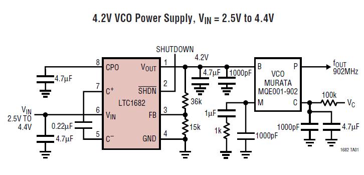
The LTC1682IS8-3.3#TR is a doubler charge pump with an internal low noise, low dropout (LDO) linear regulator. The part is designed to provide a low noise boosted supply voltage for powering noise sensitive devices such as high frequency VCOs in wireless applications. An internal doubler charge pump converts a 1.8V to 4.4V input to a boosted output, while the internal LDO regulator converts the boosted voltage to a low noise regulated output. The applications of the LTC1682IS8-3.3#TR include VCO Power Supplies in Cellular Phones, 2-Way Pagers, Wireless PCMCIA Cards, Portable Medical Instruments, Low Power Data Acquisition, Remote Transmitters.
Parametrics
LTC1682IS8-3.3#TR absolute maximum ratings: (1)VIN to Ground: -0.3V to 5V; (2)VOUT Voltage: -0.3V to 6V; (3)CPO to Ground: 10V; (4)SHDN, FILT/FB Voltage to Ground: -0.3V to (VIN + 0.3V); (5)VOUT Short-Circuit Duration: Indefinite; (6)IOUT: 90mA; (7)Operating Temperature Range; (8)Commercial: 0℃ to 70℃; (9)Extended Commercial (Note 2): -40℃ to 85℃; (10)Industrial: -40℃ to 85℃; (11)Storage Temperature Range: -65℃ to 150℃; (12)Lead Temperature (Soldering, 10 sec): 300℃; (13)Maximum Junction Temperature: 125℃.
Features
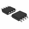
LTC1682IS8-3.3#TR features: (1)Low Output Noise: 60mVRMS (100kHz BW); (2)Adjustable or Fixed Boosted Output; (3)Adjustable Output Voltage Range: 2.5V to 5.5V; (4)Fixed Output Voltages: 3.3V, 5V; (5)Wide Input Voltage Range: 1.8V to 4.4V; (6)Uses Small Ceramic Capacitors; (7)No Inductors Required; (8)Output Current up to 50mA; (9)550kHz Switching Frequency; (10)Low Operating Current: 150mA; (11)Low Shutdown Current: 1mA; (12)Internal Thermal Shutdown and Current Limiting; (13)Available in 8-Pin MSOP and SO Packages.
Diagrams
| Image | Part No | Mfg | Description |  |
Pricing (USD) |
Quantity | ||||||
|---|---|---|---|---|---|---|---|---|---|---|---|---|
 |
 LTC1682IS8-3.3#TR |
|
IC REG MULTI CONFIG 3.3V 8SOIC |
Data Sheet |
|
|
||||||
|
LTC1682IS8-3.3#TRPBF |
|
IC REG MULTI CONFIG 3.3V 8SOIC |
Data Sheet |
|
|
||||||