Product Summary
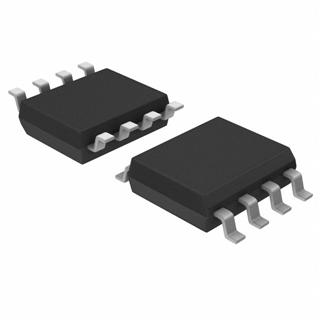
The LTC1481CS8#TR is an ultra-low power differential line transceiver designed for data transmission standard RS485 applications. It will also meet the requirements of RS422. The CMOS design offers significant power savings over its bipolar counterparts without sacrificing ruggedness against overload or ESD damage. Typical quiescent current is only 80mA while operating and less than 1mA in shutdown. The applications of the LTC1481CS8#TR include Battery-Powered RS485/RS422 Applications, Low Power RS485/RS422 Transceiver, Level Translator.
Parametrics
LTC1481CS8#TR absolute maximum ratings: (1)Supply Voltage (VCC): 12V; (2)Control Input Voltage: -0.5V to VCC + 0.5V; (3)Driver Input Voltage: -0.5V to VCC + 0.5V; (4)Driver Output Voltage: ±14V; (5)Receiver Input Voltage: ±14V; (6)Receiver Output Voltage: -0.5V to VCC + 0.5V; (7)Operating Temperature Range: 0℃ ≤ TA ≤ 70℃; (8)Lead Temperature (Soldering, 10 sec): 300℃.
Features
LTC1481CS8#TR features: (1)Low Power: ICC = 120mA Max with Driver Disabled; (2)ICC = 500mA Max with Driver Enabled, No Load; (3)Drivers/Receivers Have ±10kV ESD Protection; (4)1mA Quiescent Current in Shutdown Mode; (5)High Speed: Up to 2.5Mbits/s Data Rate; (6)Single 5V Supply; (7)–7V to 12V Common-Mode Range Permits ±7V Ground Difference Between Devices on the Data Line; (8)Thermal Shutdown Protection; (9)Power Up/Down Glitch-Free Driver Outputs Permit Live Insertion or Removal of Transceiver; (10)Driver Maintains High Impedance in Three-State or with the Power Off; (11)Up to 32 Transceivers on the Bus; (12)30ns Typical Driver Propagation Delays with 5ns Skew; (13)Pin Compatible with the LTC485.
Diagrams

| Image | Part No | Mfg | Description |  |
Pricing (USD) |
Quantity | ||||||
|---|---|---|---|---|---|---|---|---|---|---|---|---|
 |
 LTC1481CS8#TR |
 |
 IC TXRX RS485 SHTDN ULT LP 8SOIC |
 Data Sheet |

|
|
||||||
 |
 LTC1481CS8#TRPBF |
 |
 IC TXRX RS485 LOPWR W/SHTDN8SOIC |
 Data Sheet |

|
|
||||||
 (Hong Kong)

