(Hong Kong)

Product Summary
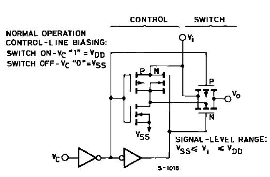
The HCF4066BE is a monolithic integrated circuits, available in 14-lead dual in-line plastic or ceramic package and plastic micropackage. The HCF4066BE is a quad bilateral switch intended for the transmission or multiplexing of analog or digital signals. It is pin-for-pin compatible with the HCF4066BE, but exhibits a much lower ON resistance. In addition, the ON resistance is relatively constant over the full input-signal range. The HCF4066BE consists of four independent bilateral switches. A single control signal is required per switch.
Parametrics
HCF4066BE absolute maximum ratings: (1)Supply Voltage, VDD: -0.5 to + 18V; (2)Input Voltage, Vi: -0.5 to VDD +0.5 V; (3)DC Input Current (any one input), II: ±10 mA; (4)Total Power Dissipation (per package), Ptot: 200mW; Dissipation per Output Transistor for Top = Full Package-temperature Range, Ptot: 100mW; (5)Operating Temperature, Top: -40 to +85℃; (6)Storage Temperature, Tstg: -65 to + 150℃.
Features
HCF4066BE features: (1)15v digital or ±7.5v peak-to-peakswitching; (2)80w typical on resistance for 15v operation; (3)switch on resistance matched to within 5w over 15v signal-input range; (4)on resistance flat over full peak to-peaksignal range; (5)high on/off output-voltage ratio: 65db typ.@ fis = 10khz, rl = 10kΩ; (6)high degree of linearity: < 0.5% distortion typ.@ fis = 1khz, vis = 5 vp-p, vdd - vss ≥ 10v, rl = 10kw; (7)extremely low off switch leakage resulting in very low offset current and high effective off resistance; 10pa typ.@ vdd – vss = 10V, ta = 25℃; (8)extremely high control input impedance (control circuit isolated from signal cir-cuit): 1012 w typ; (9)low crosstalk between switches: -50db typ.@ fis = 0.9mhz, rl = 1kΩ; (10)matched control-input to signaloutput capacitance: reduces out-; (11)put signal transients; (12)frequency response, switch on = 40mhz (typ.); (13)quiescent current specified to 20v for hcc device; (14)5V, 10V, and 15V parametric ratings input current of 100na at 18v and 25℃ for hcc device; (15)100% tested for quiescent current; (16)meets all requirements of jedec tentative standard No. 13A, ”standard specifications for description of ”b” seriescmos devices”.
Diagrams
| Image | Part No | Mfg | Description |  |
Pricing (USD) |
Quantity | ||||||||||||||||||
|---|---|---|---|---|---|---|---|---|---|---|---|---|---|---|---|---|---|---|---|---|---|---|---|---|
 |
 HCF4066BEY |
STMicroelectronics |
Analog Switch ICs Quad Bilateral Sw |
Data Sheet |
|
|
||||||||||||||||||
| Image | Part No | Mfg | Description | |
Pricing (USD) |
Quantity | ||||||||||||||||||
 |
HCF4001B |
Other |
|
Data Sheet |
Negotiable |
|
||||||||||||||||||
|
HCF4001BEY |
STMicroelectronics |
Gates (AND / NAND / OR / NOR) Quad 2-Input NOR |
Data Sheet |
|
|
||||||||||||||||||
 |
HCF4001M013TR |
|
IC GATE NOR QUAD 2INP 14-SOIC |
Data Sheet |
|
|
||||||||||||||||||
|
HCF4002B |
Other |
|
Data Sheet |
Negotiable |
|
||||||||||||||||||
|
HCF4006B |
Other |
|
Data Sheet |
Negotiable |
|
||||||||||||||||||
|
HCF4007UB |
Other |
|
Data Sheet |
Negotiable |
|
||||||||||||||||||